Wafer & Materials
Wafer
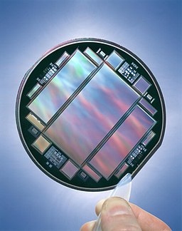
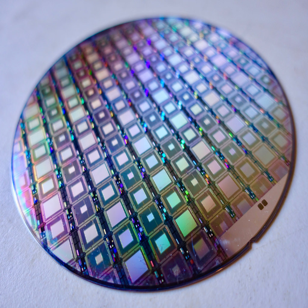
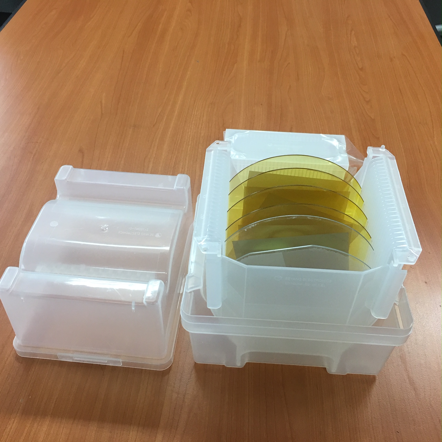
We mainly sell Silicon base substrate used in semiconductors and Sapphire base substrate used for LED.
Wafer is a substrate for manufacturing semiconductor or LED chip, and best result can be obtained by selecting appropriate substrate for device.

Silicon Wafer
| Growing method | CA |
|---|---|
| Grade | PRIME, TEST, DUMMY |
| Type | P-type(Boron), N-type(Phos, Antimony, Arsenic) |
| Orientation | <100>, <111>, <110> |
| Resistivity | 0.001 ~ 0.1Ωcm, 1 ~ 30Ωcm, 100 ~ 10000Ωcm |
| Thickness | 275±25µm, 525±25µm, 675±25µm, 725±25µm, 750±25µm |
| Surface | SSP & DSP |

Sapphire Wafer
| Growing method | KY, HEM |
|---|---|
| Orientation | C-axis[0001] |
| Thickness | 430±10µm, 660±10µm, 1300±10µm |
| Surface | Front side : Epi-ready, PSS surface |

* For the Sliicon wafer, it can be supplied with thickness from 50μm by adding CMP process upon the request.
* TTV (Total Thickness Variation): <15μm, but can be processed to a minimum of 2μm by adding CMP process
* Produce SOI (Silicon On Insulator), SOG (Silicon On Glass), SOQ (Silicon On Quartz)
Chemical
Various chemicals are used in semiconductor manufacturing processes such as cleaning and etching.

Ingredient : NH4OH / H2O2 / H2O
Main use : Remove particle
It is mixed with ammonia (NH4OH), hydrogen peroxide (H2O2) and DI (H2O) at a ratio of 1: 1: 5 and cleaning is carried out at 75 ~ 90℃. H2O2 is separated into H2O and O2, Allow the substances to dissolve well in water.
It is mainly used to remove particles and remove residual organic impurities such as Au, Ag, Cu, Ni, Cd, Zn, Co and Cr on the surface.
Ingredient : HCl / H2O2 / H2O
Main use : Metal impurity removal
The process is performed at 75 ~ 85℃ by mixing hydrochloric acid (HCl), water (H2O2) and DI (H2O) at a ratio of 1: 1: 5.
The reason for using 75 to 85°C is that the cleaning liquid can be sufficiently activated and the decomposition of hydrogen peroxide does not progress rapidly. After cleaning, a chemical oxide film of about 15 Å is formed on the surface, and the surface shows a hydrophilic property. It is effective to remove metal contaminants and alkali metals.
Ingredient : H2SO4 / H2O2
Main use : Organic matter removal
Sulfuric acid(H2SO4) and hydrogen peroxide (H2O2) at a ratio of 4: 1, and proceeding at 90 to 130°C.
It is used to remove organic contaminants on the wafer surface, effectively removing heavy organic contaminants such as photoresist, forming a chemical oxide film after cleaning, and the substrate surface showing hydrophilic properties.
| Process | Ingredient | Main use |
|---|---|---|
| Etching | H3PO4 / H2O | Si3N4 Etching |
| HNO3 / HF / H2O(/CH3COOH) | Si Etching | |
| H3PO4 / HNO3 / CH3COOH / H2O | Ai Etching | |
| NH4F / HF / H2O | SiO2 Etching | |
| Resist Peeling Liquid | Peel the resist | |
| Polymer Removal Liquid | Removal of Etching product | |
| Cleaning Liquid after CMP | Removal of slurry metal particles | |
| Developer (TMAH) | Develop the resist |
| # | Product Descriptions | Unit |
|---|---|---|
| 1 | Hydrochloric Acid(HCl) | Gal |
| 2 | Ammonia(NH4OH) | Gal |
| 3 | Nitric Acid(HNO3) | Gal |
| 4 | Hydrogen Peroxide(H2O2) | Gal |
| 5 | Nano-strip2x | Gal |
| 6 | IPA | Gal |
| 7 | IPA | 20L |
| 8 | Sulfuric Acid(H2SO4) | 20L |
| 9 | Acetone | 20L |
| 10 | BOE 20:1 | 20L |
| 11 | BOE 6:1 | 20L |
| 12 | Printing Emulsion Remover (ASP-S202) | 20L |